Open source analog integrated circuit flow on Skywater 130nm
Getting started with analog integrated circuit design is hard. For most technologies (28 nm TSMC, Globalfoundries 65 nm) you need to sign an Non Disclosure Agreement (NDA), and as a private person, I’m not sure it’s possible. As such, the fact that there is now an open source technology sky130nm is fantastic.
If you find errors/bugs in this “tutorial”, then fork, fix, and send me a PR.
Table of Contents
- Tools
- Make IP files
- Current mirror
- Draw Schematic
- Typical SPICE simulation
- Corner SPICE simulation
- Draw Layout
- Layout verification
- Extract layout parasitics
- Simulate with layout parasitics
- Gotchas
Tools
Assumed knowledge
I really hope that you’re comfortable in the terminal and working with files/directories. If you’ve never used the terminal before, then you neeed to learn that first before you continue. Google “getting started with terminal”.
Operating system
I wrote this tutorial on MacOS, and it should translate to linux.
Windows is a different story. I would strongly recommend you install Windows Subsystem for Linux and MobaXterm to get the GUI.
On Windows 11 I think WSL includes a GUI, but I have not tried that.
You need to get comfortable in a unix based system if you plan to have a career in integrated circuit design.
Make project folder
Navigate to a place where you will store your files. I have the following setup.
$HOME/pro  # Automatically synced to my one-drive
$HOME/lpro # Where I store all my own git repos that I know I can loose
For example:
mkdir lpro
cd lpro
mkdir rply_ex0
cd rply_ex0
For the rest of the tutorial, I’ll assume you’ll use lpro/rply_ex0 as the project folder.
Open source tools
We first ran this tutorial in the spring of 2023. If you check the 1.0.1 tag , you’ll find the post from that time.
The main thing we learned was, in theory, a docker image is a fast way to start, in practice, it was not. Lot’s of issues with Windows 11, X-server etc.
I would recommend you install all tools locally. Follow the description at Getting Started
Even if you have all the open source tools installed, you do need to install cicsim and
cicconf (Unless you just did while reading the Getting Started link)
python3 -m pip install cicsim cicconf
Make cicconf config file
Open a new file called config.yaml in your favorite
text editor, and add it to the rply_ex0 directory.
options:
  template:
    ip: tech_sky130B/cicconf/ip_template.yaml
  project: rply
  technology: sky130nm
cpdk:
  remote: git@github.com:wulffern/cpdk.git
  revision: 0.1.1
tech_sky130B:
  remote: git@github.com:wulffern/tech_sky130B.git
  revision: 0.1.0
Get the tech library, and necessary files.
In rply_ex0:
cicconf clone --https
Make IP files
Initialize new IP
The technology library includes a template to generate
IPs (make directories, make a xschem view etc). Have
a look inside tech_sky130B/cicconf/ip_template.yaml to
see what it does.
In rply_ex0:
cicconf newip ex0
Add remote repository
You don’t have to add a remote, but it’s a nice way to collaborate with others.
There are at least two options. You need to decide what you want to do.
Use my remote
If you want to skip parts of this tutorial, for example, you already know how to draw schematics in Xschem, you can connect to my remote. My repository contains the files at different stages during this tutorial, and enables you to skip parts.
cd rply_ex0_sky130nm
git branch local
git remote add origin \
 https://github.com/wulffern/rply_ex0_sky130nm.git
git pull
With my remote you can for example fast forward to tags. You can see the tags below.
| Tag | Status | Comment |
|---|---|---|
| 0.0.0 | Make files and directories | |
| 0.1.0 | Fix readme | |
| 0.2.0 | Made schematic | |
| 0.3.0 | Typical simulation | |
| 0.4.0 | Corner simulation | |
| 0.5.0 | Made layout | |
| 0.6.0 | DRC/LVS clean | |
| 0.7.0 | Extracted parasitics | |
| 0.8.0 | Simulated parasitics | |
| 0.9.0 | Updated README with simulation results | |
| 1.0.0 | All done |
For example, checkout the initial tag:
git checkout 0.1.0
ls -1RG
Or checkout the final design:
git checkout 1.0.0
ls -1RG
You can see the number of files are very different.
Checkout the local tag before you proceed.
git checkout local
Since you have a new repository, it does not have the same history as mine, so lets fix that with a rebase
git rebase 0.0.0
Use your own remote
Create a repository with the same name on your choosen git vendor (for example github)
cd rply_ex0_sky130nm
git remote add origin \
 git@github.com:<your user name>/rply_ex0_sky130nm.git
Edit README.md
Open README.md in your favorite text editor and make necessary changes.
Familiarize yourself with the Makefile and make
I write all commands I do into a Makefile. There is nothing special with a Makefile, it’s just what I choose to use 20 years ago. I’m not sure I’d choose something different now.
cd work
make
Take a look inside the file called Makefile.
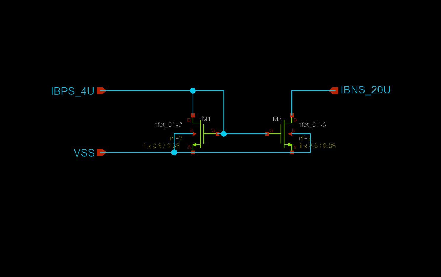
Current mirror
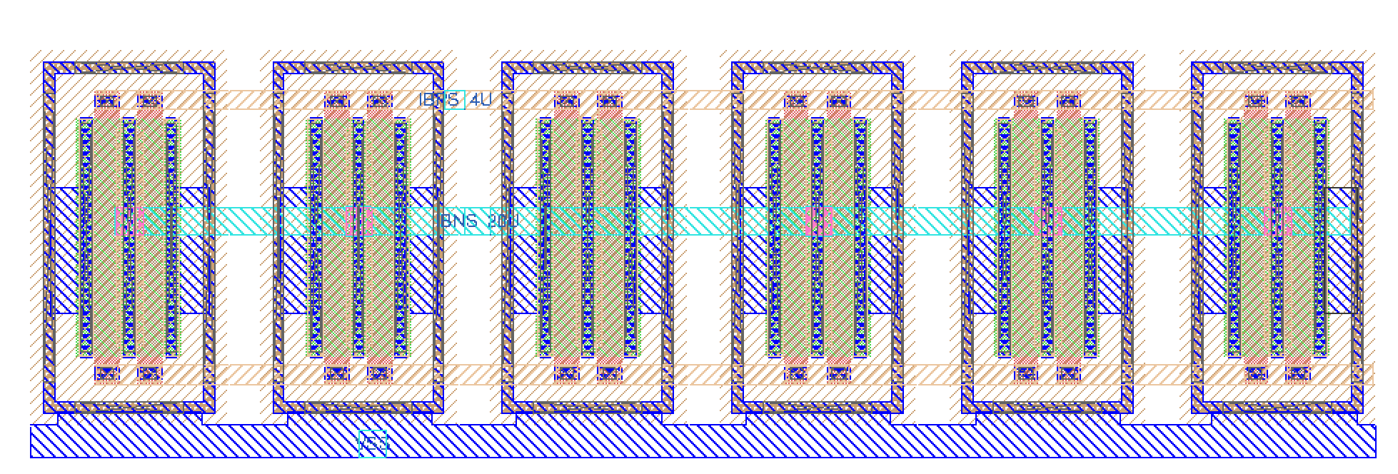
The block we’ll make is a current mirror with a 1 to 5 scaling. The design files will be
| What | Lib/Folder | Cell/Name |
|---|---|---|
| Schematic | RPLY_EX0_SKY130NM | RPLY_EX0.sch |
| Layout | RPLY_EX0_SKY130NM | RPLY_EX0.mag |
The signal interface will be
| Signal | Direction | Domain | Description |
|---|---|---|---|
| IBPS_4U | Input | VDD_1V8 | Input bias current |
| IBNS_20U | Output | VDD_1V8 | Output current |
| VSS | Input | Ground |
| Parameter | Min | Typ | Max | Unit |
|---|---|---|---|---|
| Technology | Skywater 130 nm | |||
| AVDD | 1.7 | 1.8 | 1.9 | V |
| IBNS_20U | 16 | 21 | 27 | uA |
| Temperature | -40 | 27 | 125 | C |
Draw Schematic
A schematic is how we describe the connectivity, and the types of devices in an analog circuit. The open source schematic editor we will use is XSchem.
Fun fact: The schematic files are text files, open the one called *.sch in your favorite text editor and have a look.
All commands (except simulation commands) must be started from work/
In the work/ folder there are startup files for Xschem (xschemrc) and Magic (.magicrc). They tell the tools where to find the process design kit, symbols, etc. At some point you probably need to learn those also, but I’d wait until you feel a bit more comfortable.
Open the schematic:
xschem -b ../design/RPLY_EX0_SKY130NM/RPLY_EX0.sch &
Add Ports
Add IBPS_4U and IBPS_20U ports, the P and N in the name signifies what transistor the current comes from. So IBPS must go into a diode connected NMOS, and N will be our output, and go into a diode connected PMOS somewhere else.
Add transistors
Use ‘Shift-I’ to open the library manager. Use the “sky130B/libs.tech/xschem” path. Open the “sky130_fd_pr” library. Find nfet_01v8.sym and place in your schematic.
Select the transistor by clicking on it, press ‘q’ to bring up the properties. Set L=0.36, W=3.6, nf=2 and press OK.
Select the transistor and press ‘c’ to copy it, while dragging, press ‘shift-f’ to flip the transistor so our current mirror looks nice. ‘shift-r’ rotates the transistor, but we don’t want that now.
Press ESC to deselect everything
Select ports, and use ‘m’ to move the ports close to the transistors.
Press ‘w’ to route wires.
Use ‘shift-z’ and z, to zoom in and out
Use ‘f’ to zoom full screen
Remember to save the schematic
Netlist schematic
Check that the netlist looks OK
In work/
make xsch
cat xsch/RPLY_EX0.spice
Typical corner SPICE simulation
I’ve made cicsim that I use to run simulations (ngspice) and extract results
Setup simulation environment
Navigate to the rply_ex0_sky130nm/sim/ directory.
Make a new simulation folder
cicsim simcell  RPLY_EX0_SKY130NM \
 RPLY_EX0 ../tech/cicsim/simcell_template.yaml
I would recommend you have a look at simcell_template.yaml file to understand what happens.
Familiarize yourself with the simulation folder
I’ve added quite a few options to cicsim, and it might be confusing. For reference, these are what the files are used for
| File | Description |
|---|---|
| Makefile | Simulation commands |
| cicsim.yaml | Setup for cicsim |
| summary.yaml | Generate a README with simulation results |
| tran.meas | Measurement to be done after simulation |
| tran.py | Optional python script to run for each simulation |
| tran.spi | Transient testbench |
| tran.yaml | What measurements to summarize |
The default setup should run, so
cd RPLY_EX0
make typical
Modify default testbench (tran.spi)
Delete the VDD source
Add a current source of 4uA, and a voltage source of 1V to IBNS_20U
IBP 0 IBPS_4U dc 4u
V0  IBNS_20U 0 dc 1
Save the current in V0 by adding i(V0) to the save statement in the testbench
Modify measurements (tran.meas)
Add measurement of the current and VGS. It must be added between the “MEAS_START” and “MEAS_END” lines.
let ibn = -i(v0)
meas tran ibns_20u find ibn at=5n
meas tran vgs_m1 find v(ibps_4u) at=5n
Run simulation
make typical
and check that the output looks okish.
If you get wierd results, then check the
port order in the tran.spi compared to the ../work/xsch/RPLY_EX0.spice
file. I’ve seen different versions of Xschem netlist the schematic differently.
Often, it’s the measurement that I get wrong, so instead of rerunning simulation every time I’ve added a “–no-run” option to cicsim. For example
make typical OPT="--no-run"
will skip the simulation, and rerun only the measurement. This is why you should split the testbench and the measurement. Simulations can run for days, but measurement takes seconds.
You should notice that the current is not 20uA. We need to fix the schematic to make that happen. Change the instance name of M2 to “M2[4:0]”, and rerun typical simulation. Remember to save the schematic.
Modify result specification (tran.yaml)
Add the result specifications, for example
ibn:
  src:
    - ibns_20u
  name: Output current
  min: -20%
  typ: 20
  max: 20%
  scale: 1e6
  digits: 3
  unit: uA

vgs:
  src:
    - vgs_m1
  name: Gate-Source voltage
  typ: 0.6
  min: 0.3
  max: 0.7
  scale: 1
  digits: 3
  unit: V
Re-run the measurement and result generation
make typical OPT="--no-run"
Open result/tran_Sch_typical.html
Check waveforms
Start Ngspice
ngspice
Load the results, and view the vgs
In ngspice
load output_tran/tran_SchGtAttTtVt.raw
plot v(ibps_4u)
plot i(v0)
Based on the waveform we can see that maybe the voltage and current is not completely settled at 5 ns.
Change the measurement to occur at 9.5ns
All corners SPICE simulations
All commands should be run in sim/RPLY_EX0
Analog circuits must be simulated for all physical conditions, we call them corners. We must check high and low temperature, high and low voltage, all process corners, and device-to-device mismatch.
For the current mirror we don’t need to vary voltage, since we don’t have a VDD.
Remove Vh and Vl corners (Makefile)
Open Makefile in your favorite text editor.
Change all instances of “Vt,Vl,Vh” and “Vl,Vh” to Vt
Run all corners
To simulate all corners do
make typical etc mc
where etc is extreme test condition and mc is monte-carlo.
Wait for simulations to complete.
Modify measurements to check settling
Let’s say we want to check if the current has settled in our transient. We could extract the current at 9.0 ns and check that it’s roughly the same.
Add the following line to tran.meas
meas tran ibns_20u_9n find ibn at=9n
And add the parameter to tran.yaml
ibn:
  src:
    - ibns_20u
    - ibns_20u_9n
Now, as you saw, the simulations take quite a while, so we don’t want to rerun that. Instead do
make typical etc mc OPT="--no-run"
Get creative with python
If you’re lazy, like me, then you don’t want to spend time checking all the 9.5 ns numbers versus the 9 ns numbers. I’d much rather tell the computer how to do that.
It might be possible to do in ngspice, but sometimes a more complex tool is easier.
Open tran.py in your favorite editor, try to read and understand it.
The name parameter is the corner currently running, for example tran_SchGtAmcttTtVt.
The measured outputs from ngspice will be added to tran_SchGtAmcttTtVt.yaml
Delete the “return” line.
Add the following line
# Do something to parameters
obj["ibn_settl_err"] = \
  obj["ibns_20u"] - obj["ibns_20u_9n"]
Add the error to the result spec tran.yaml
err:
  src:
    - ibn_settl_err
  name: Current settling error
  typ: 0
  min: -2
  max: 2
  scale: 1e9
  digits: 3
  unit: nA
Re-run measurements to check the python code
make typical etc mc OPT="--no-run"
Generate simulation summary
Run
make summary
Install pandoc if you don’t have it
Run
pandoc -s -t slidy README.md -o README.html
to generate a HTML slideshow that you can open in browser. Open the HTML file.
Viewing results without GUI browser
If your on a system without a browser, or indeed a GUI, then it’s possible to view the results in the terminal.
Check if lynx is installed, if it’s not installed, then
On linux
sudo apt-get install lynx
On Mac
brew install lynx
Then
lynx README.html
Think about the results
From the corner and mismatch simulation, we can observe a few things.
- The typical value is not 20 uA. This is likely because we have a M2 VDS of 1 V, which is not the same as the VDS of M1. As such, the current will not be the same.
- The statistics from 30 corners show that when we add or subtract 3 standard deviation from the mean, the resulting current is outside our specification of +- 20 %. I’ll leave it up to you to fix it.
Draw Layout
A foundry (the factory that makes integrated circuits) needs to know how we want them to create our circuit. So we need to provide them with a “layout”, the recipe, or instruction, for how to make the circuit. Although the layout contains the same components as the schematic, the layout contains the physical locations, and how to actually instruct the foundry on how to make the transistors we want.
Open Magic VLSI
magic &
Navigate to design directory
cd ../design
cd RPLY_EX0_SKY130NM
load RPLY_EX0.mag
Now brace yourself, Magic VLSI was created in the 1980’s. For it’s time it was extremely modern, however, today it seems dated. However, it is free, so we use it.
Magic VLSI
Try google for most questions, and there are youtube videos that give an intro.
Default magic start with the BOX tool. Mouse left-click to select bottom corner, left-click to select top corner.
Press “space” to select another tool (WIRING, NETLIST, PICK).
Type “macro help” in the command window to see all shortcuts
| Hotkey | Function |
|---|---|
| v | View all |
| shift-z | zoom out |
| z | zoom in |
| x | look inside box (expand) |
| shift-x | don’t look inside box (unexpand) |
| u | undo |
| d | delete |
| s | select |
| Shift-Up | Move cell up |
| Shift-Down | Move cell down |
| Shift-Left | Move cell left |
| Shift-Right | Moce cell right |
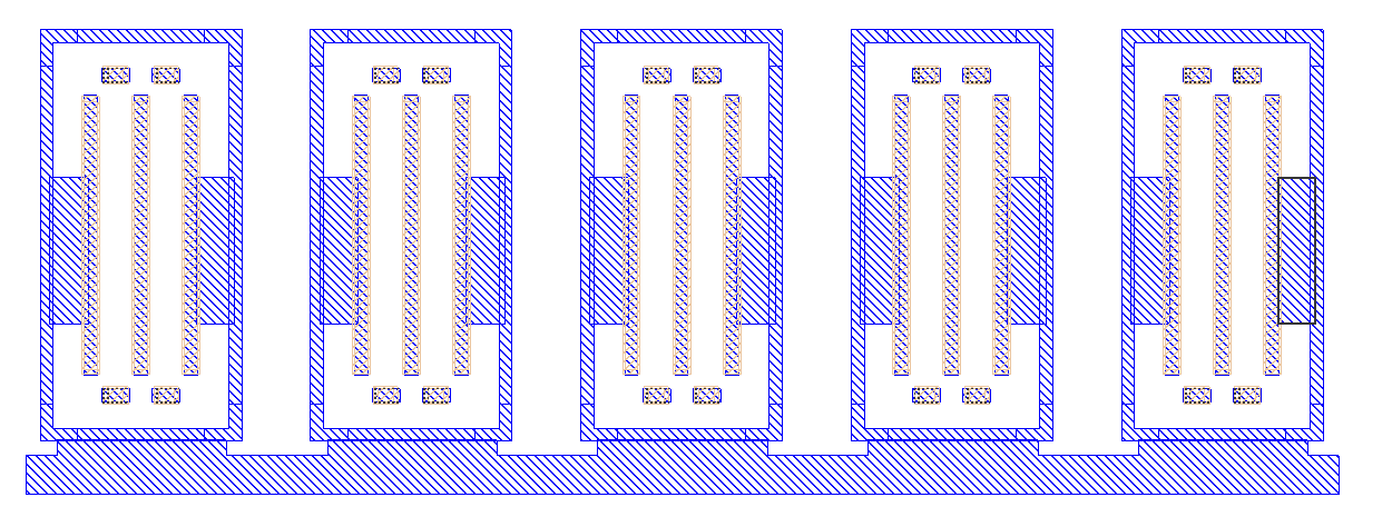
Add transistors
In the Window menu, turn grid on, set grid 0.5 um and turn on snap-to grid.
Select “Devices 1 - NMOS”. Match the parameters to schematic (W=3.6, L=0.36, fingers=2)
Unexpand, so it’s possible to select the device (shift-x)
Place cursor over the device and select (s)
Move cursor to somewhere else, and copy (c), it will then snap to grid.
Select the old device, and delete (d).
Copy 4 more devices for M2.
Add Ground
In the command window, type
see no *
see locali
see m1
Select a 0.5 um box below the transistors and paint the rectangle (middle click on locali)
Change grid to 0.1 um.
Connect guard rings to ground. Select a smaller box between guardring and the ground rectangle.
Select the rectangle, and copy to the other transistors
Connect the sources to ground.
Route Gates
All the gates are connected, so we can enter use the wire mode
see no locali
It seems like the device generator adds too small m1 around the gate, so add a rectangle.
Press “space” to enter wire mode. Left click to start a wire, and right click to end the wire.
The drain of M1 transistor needs a connection to from gate to drain. We do that for the middle transistor.
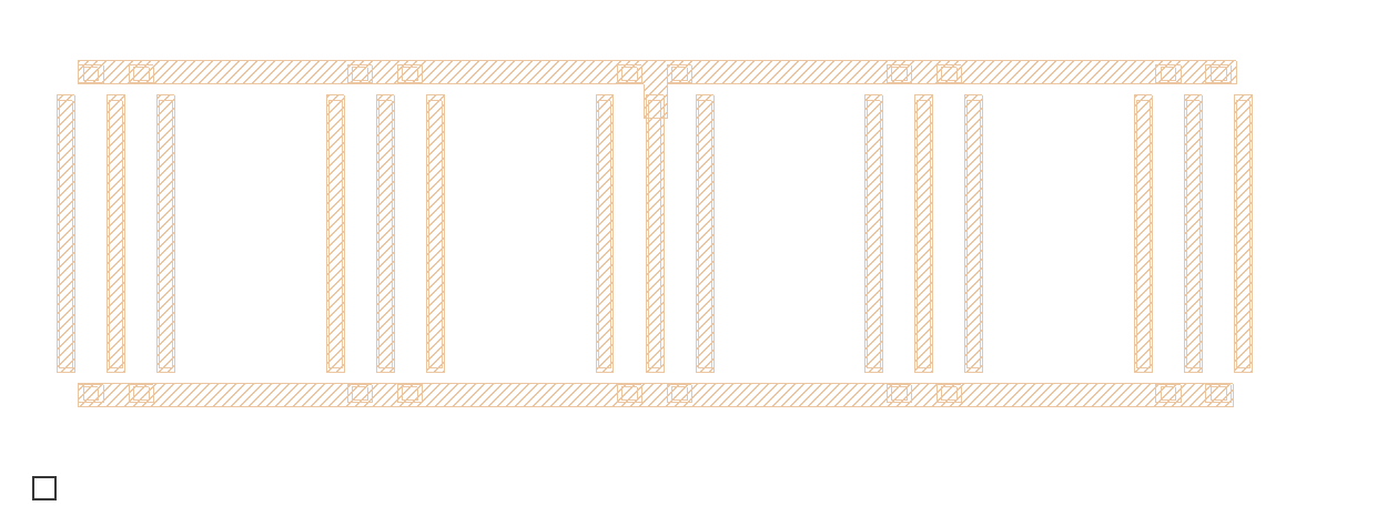
Drain of M2
Select a box on the left most transistor drain. Paint m1.
Unexpand all, use the wire tool to draw connections for the drains.
To add vias you can do “shift-left” to move up a metal, and “shift-right” to go down.
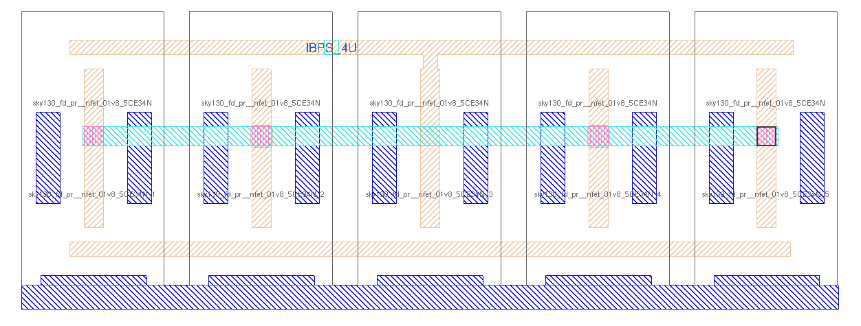
Add labels
Select a box on a metal, and use “Edit->Text” to add labels for the ports.
Layout verification
The DRC can be seen directly in Magic VLSI as you draw.
To check layout versus schematic navigate to work/ and do
make xsch xlvs
And you should see that it’s incorrect. I forgot one transistor of the current mirror, M2 was 5 devices.
Add the fith transistor and try again. It should still be incorrect.
Turns out that the Xschem interpretation of width is different than in Magic VLSI.
In xschem “W=3.6, nf=2” means that the device is actually 3.6 um wide, but has two fingers. In Magic “W=3.6, nf=2” means that the device is 7.2 um wide, and has fingers of 3.6 um.
The easiest way to fix it is to modify the schematic to match the layout.
Open the schematic, select M1, press q, and change “W=7.2”. Do the same for M2.
Now the layout should match the schematic.
Extract layout parasitics
With the layout complete, we can extract parasitic capacitance.
make lpe
Check the generated netlist
cat lpe/RPLY_EX0_lpe.spi
Simulate with layout parasitics
Navigate to sim/RPLY_EX0. We now want to simulate the layout.
The default tran.spi should already have support for that.
Open the Makefile, and change
VIEW=Sch
to
VIEW=Lay
Typical simuation
Run
make typical
The simulation might not look right.
Open the work/lpe/RPLY_EX0_lpe.spi and work/xsch/RPLY_EX0.spice and have a look at the .subckt line.
For me, the ports were not the same order, which makes the simuation fail.
To fix it, open design/RPLY_EX0_SKY130NM/RPLY_EX0.mag in your favorite text editor.
Yes, the layout file is a text file!
Take a look towards the bottom, you’ll see
flabel metal1 4460 ... IBPS_4U
port 1 nsew
flabel locali 4200 ... VSS
port 2 nsew
flabel metal2 4520 ... IBNS_20U
port 3 nsew
Change the numbers so we get the same port order as the schematic
flabel metal1 4460 ... IBPS_4U
port 2 nsew
flabel locali 4200 ... VSS
port 1 nsew
flabel metal2 4520 ... IBNS_20U
port 3 nsew
Open a new terminal, navigate to work/ and extract the parasitics again
make lpe
Check the work/lpe/RPLY_EX0_lpe.spi again.
Run typical simulation.
Observer that now the difference between “ibps_20u” and “ibps_20u_9n” is a bit large.
Check the current waveform. Change the transient simulation to run a bit longer, and extract a bit later. 19.5 ns seem to work.
Corners
Navigate to sim/RPLY_EX0. Run all corners again
make all
Simulation summary
Open summary.yaml and add the layout files.
      - name: Lay_typ
        src: results/tran_Lay_typical
        method: typical
      - name: Lay_etc
        src: results/tran_Lay_etc
        method: minmax
      - name: Lay_3std
        src: results/tran_Lay_mc
        method: 3std
Open the README.md and have a look a the results.
You can also have a look at the rendered page
Gotchas
- If you have not resimulated the schematic, then you’re comparing apples to oranges since the schematic had W=3.6
- In the extracted layout the ad, as, etc looks funky, I don’t understand why they are zero
- One of reasons the simulation is slow is that ngspice needs to load about 50 MB of spice files (the skywater models). They could run faster if we only loaded what is necessary, but that’s a bit more work.